Microcontrollers (MCUs) are at the heart of countless embedded systems, driving innovations in industries like consumer electronics, automotive, and industrial applications. This article provides an overview of these powerful devices, highlighting their key features and practical uses.
What is a Microcontroller?
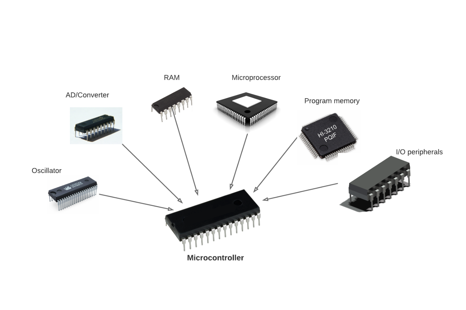
It is an integrated circuit designed to perform specific tasks within a system. It combines a processor, memory, and peripheral devices on a single chip, making it ideal for applications that require low power, cost efficiency, and space optimization. They are commonly used in appliances, sensor monitoring, and device communication.
For instance, a car contains multiple MCUs that manage different systems, such as the anti-lock braking system, traction control, fuel injection, and suspension. These MCUs communicate with each other to coordinate actions, ensuring proper system performance. Some may interact with a central computer, while others communicate directly with nearby MCUs. They exchange data through their I/O peripherals and process it to carry out specific tasks efficiently.

A microcontroller is a complete system embedded within a single integrated circuit (IC), typically containing a processor, program memory, RAM, input/output pins, and various other components. (Source: Circuit Basics)
How Do MCUs Work?
These devices manage specific functions within embedded systems. They process data from input/output (I/O) peripherals and use their central processor to interpret the information. Data is temporarily stored in memory, where the processor accesses and applies it using predefined instructions. The results are then communicated through I/O peripherals, triggering the appropriate response.
In many systems, multiple MCUs work together to control various functions. For example, in a car, MCUs manage individual systems such as braking, fuel injection, and suspension, all communicating with each other or a central computer to ensure smooth operation.
Anatomy of a MCU
- Central Processing Unit (CPU): The core of the microcontroller, responsible for executing instructions. It can be 8-bit, 16-bit, or 32-bit, depending on performance requirements.
- Memory: Microcontrollers use two types of memory—program memory for storing code and data memory for temporary storage. Flash memory is typically used for program storage, while RAM stores data.
- Input/Output (I/O) Ports: These allow the microcontroller to interface with external devices like sensors and actuators.
- Peripherals: peripherals like analog-to-digital converters (ADCs), timers, and communication interfaces such as UART, SPI, and I2C to handle specific tasks.
Understanding Microcontroller Architectures
They are categorized by data bus width, which defines how much data is processed per cycle:
8-bit microcontrollers are built with an 8-bit data bus, meaning they can process 8 bits (or 1 byte) of data at a time. These control units are ideal for simple applications where low power consumption and cost are the top priorities. They are often used in devices where only basic tasks need to be managed, such as in home appliances and basic control systems.
Examples: Remote controls, basic motor controllers, and small consumer devices like coffee makers or washing machines. These applications require simple decision-making logic, such as turning motors on or off based on sensor inputs.
16-bit microcontrollers have a data bus that allows for the processing of 16 bits (or 2 bytes) at once. This wider bus offers better performance than 8-bit architectures, enabling more complex tasks while still keeping power consumption relatively low. They are commonly used in applications where more precision or faster processing is required, but cost and power efficiency are still important.
Examples: Automotive applications, such as digital dashboards or engine control units (ECUs), and industrial systems like temperature controllers or automation systems that require a balance between performance and efficiency.
The 32-bit microcontrollers are designed for high-performance applications, with the ability to process 32 bits of data in a single cycle. These microcontrollers offer significant processing power, faster speeds, and can handle more complex instructions. However, they also consume more power and are typically more expensive than their 8-bit or 16-bit counterparts. They are ideal for applications that require intensive computation, data processing, and multi-tasking.
Examples: Advanced robotics, IoT devices that require real-time data processing, medical devices, and smart home hubs. In these applications, the microcontroller handles complex algorithms, manages large volumes of sensor data, and performs multiple tasks simultaneously.
Essential Components of a Microcontroller
1. Central Processing Unit (CPU)
The CPU is the “brain” of the microcontroller, responsible for executing instructions from the program memory. It processes data, performs arithmetic and logical operations, and controls other components based on the tasks it needs to complete. The performance of a microcontroller largely depends on the CPU’s processing speed and architecture (8-bit, 16-bit, or 32-bit).
2. Memory
- Program Memory (Flash/ROM): Stores the microcontroller’s software (firmware) permanently, even when power is off. Flash memory is commonly used, as it allows for rewritable and upgradable firmware.
- Data Memory (RAM): Used for temporarily storing data during program execution. RAM holds variables, sensor data, and intermediate processing results while the microcontroller operates.
3. Input/Output (I/O) Ports
I/O ports are the microcontroller’s interface to the outside world. They allow the microcontroller to communicate with external devices such as sensors, switches, and actuators. These ports can be configured as input (receiving data) or output (sending data) to control or read from external components like motors, LEDs, or displays.
4. Peripherals
Peripherals are built-in hardware components that handle specific tasks:
- Timers/Counters: Track time intervals, manage events, and generate time delays.
- Communication Interfaces (UART, SPI, I2C): Facilitate data exchange between the microcontroller and other devices, such as other microcontrollers, computers, or sensors.
- Analog-to-Digital Converters (ADC): Convert analog signals (e.g., from sensors) into digital values for the microcontroller to process.
5. Clock Generator
The clock generator supplies the timing signal that drives the CPU and other components. The clock speed determines how quickly instructions are processed. Many systems allow for adjusting the clock speed to balance performance and power consumption.
6. Interrupt Controller
The interrupt controller allows the microcontroller to respond quickly to important events, such as a sensor detecting a change or a button being pressed, without continuously checking the inputs. Interrupts can temporarily pause the main program to handle urgent tasks, improving efficiency and response time.
Microcontroller Applications: Detailed Insights and Examples
They serve as the backbone for numerous modern applications. Below are some detailed use cases across different industries:
Home Automation
MCUs are widely used in smart home devices, controlling everything from lighting systems to security features. They can receive input from sensors, process the data, and take appropriate actions, such as adjusting the thermostat or turning off lights.
Example: In a smart thermostat, a microcontroller processes temperature sensor data and controls the HVAC system to maintain a comfortable environment. Similarly, in smart lighting systems, MCUs automate lighting based on motion detection or voice commands.

Robotics
Robots, both simple and complex, rely on MCUs for their core functions. These include controlling motors, processing sensor data, and handling communication between different parts of the system. Embedded processors help execute tasks like movement control and object detection, allowing robots to perform precise functions.
Example: A line-following robot uses MCUs to process data from infrared sensors and adjust motor speeds, ensuring the robot follows a designated path. In more advanced robotics, MCUs control robotic arms used in manufacturing for tasks such as welding or assembling products.
Wearables
Wearable devices, such as fitness trackers and smartwatches, are powered by MCUs. They gather and process data from sensors like accelerometers and heart rate monitors, providing real-time feedback to users.
Example: A fitness tracker utilizes a microcontroller to measure physical activity through an accelerometer and calculates steps, calories burned, or heart rate. It manages data processing, power consumption, and wireless communication with smartphones.
Automotive Systems
In modern vehicles, MCUs are used to manage various systems such as engine control, braking, air conditioning, and safety features like airbags and anti-lock braking systems (ABS). These systems rely on MCUs to operate efficiently and ensure vehicle safety.
Example: The Engine Control Unit (ECU) in a car is powered by a microcontroller that monitors sensors related to fuel consumption, air intake, and exhaust. Based on this data, the ECU adjusts the engine’s fuel injection, ensuring optimal performance and reduced emissions. Another example is the use of MCUs in controlling the deployment of airbags during a collision.
Environmental monitoring system
MCUs are essential in environmental monitoring systems, where they gather data from sensors measuring parameters like temperature, humidity, air quality, and soil moisture. These systems can monitor real-time conditions and trigger actions such as turning on ventilation or irrigation systems.
Example: A weather station uses MCUs to process sensor data on temperature, humidity, and wind speed. The embedded controller collects this information, stores it, and transmits it to a central server for analysis or local display. Similarly, air quality monitors use them to detect harmful pollutants and alert users when levels become unsafe.
 Industrial Automation
MCUs play a significant role in automating industrial processes. They are embedded in machines and control systems to manage tasks like motor control, temperature regulation, and monitoring production lines.
Example: In a factory assembly line, MCUs control robotic arms that perform repetitive tasks such as picking, placing, or welding parts. They monitor sensors to ensure precision and prevent errors, enhancing overall efficiency.
Microcontrollers vs. Microprocessors
The main difference between these devices lies in their functionality. Microcontrollers are designed for specific tasks, integrating sensors and actuators, while microprocessors focus on computation and require external peripherals like RAM. The former is more energy-efficient and cost-effective, making them ideal for embedded systems. (Find more)
Introducing Asterix – A Project by Hyphen Deux
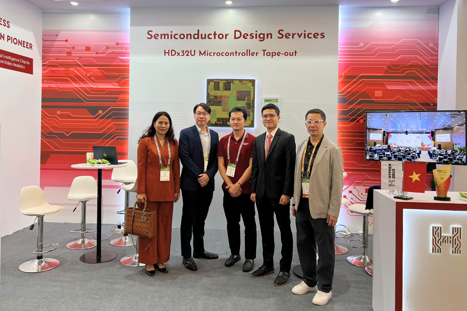
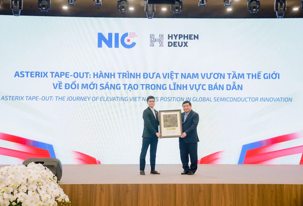
Hyphen Deux proudly presents Asterix, a high-performance microcontroller tailored for IoT and industrial applications. Powered by the ARM Cortex-M33 core with FPU and TrustZone, Asterix is designed to deliver secure, cost-effective, and energy-efficient solutions. Its advanced analog peripherals, including a 12-bit ADC and DAC, make it perfect for a range of industries, from automotive to industrial and consumer IoT.





 To reach these milestones, Vietnam will implement the strategy in three phases, starting from 2024 to 2030, with a strong focus on attracting foreign investment. The country plans to capitalize on its geopolitical stability and skilled workforce to draw international investors and position itself as a key global hub for semiconductor talent.
 In the second phase, from 2030 to 2040, Vietnam aims to become a global electronics and semiconductor powerhouse. The country plans to establish a network of 200 chip design firms, two production plants, and 15 packaging and testing facilities to advance its autonomy in chip design and production technologies.
 In the final phase, running from 2040 to 2050, Vietnam aims to rank among the world’s top semiconductor-producing nations. The plan calls for the establishment of 300 chip design companies, three semiconductor manufacturing plants, and 20 packaging and testing facilities, further enhancing the country’s self-sufficiency in chip research and development.

 Industrial Automation
 To ensure the success of this initiative, the city plans to collaborate with universities, research institutions, and international experts to train microchip engineers. With the newly established $5 million fund, the city will focus on upskilling approximately 6,000 microchip engineers per year in semiconductor design and related fields. Training courses will be offered for at least 1,200 participants annually, with support from 2-3 international experts.
 Navigating Challenges, Embracing Growth
 Pros:
Pros: Pros:
Pros:



![[Webinar] 2025 Semiconductor Supply Chain Outlook](https://hyphendeux.com/wp-content/uploads/2024/08/Picture-for-website-4-1024x683.png)