06 Key Stages of Semiconductor Manufacturing: Challenges & Growth
The semiconductor manufacturing process is a highly intricate series of steps that transform raw materials into advanced electronic devices. This journey typically encompasses six major stages: wafer fabrication, patterning, doping, deposition, etching, and wafer assembly, testing, packaging (ATP). Each phase brings its own set of unique challenges but also presents substantial opportunities for innovation, cost reduction, and scalability. In an industry where progress is driven by efficiency and precision, overcoming these challenges can lead to significant growth and technological breakthroughs that have the potential to reshape industries worldwide.
Contents
Manufacturing Process Overview: The Path from Wafer to Device

Major processes in semiconductor manufacturing
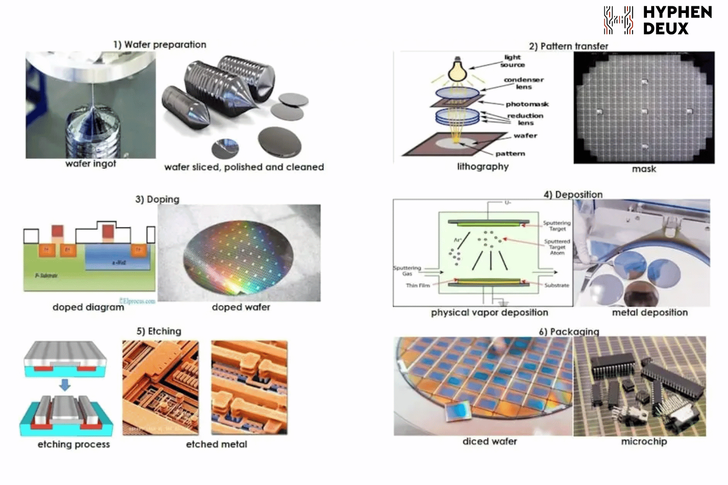
Major processes in semiconductor wafer fabrication: 1) wafer preparation, 2) pattern transfer, 3) doping, 4) deposition, 5) etching, and 6) packaging.
The semiconductor manufacturing process can be broken down into several essential steps. Each stage demands a high level of precision and advanced technological solutions:
1. Wafer Preparation
The journey begins with the selection of a silicon wafer, the foundational material for semiconductor devices. This wafer undergoes meticulous cleaning and polishing to create an ideal substrate for electronic components. The quality of this initial preparation directly impacts the subsequent stages of the process.
2. Patterning
Photolithography, the critical patterning stage, is where the design of the semiconductor is transferred onto the wafer. This involves applying a thin layer of photoresist and using ultraviolet light to transfer the pattern onto the wafer. The ability to etch smaller, more intricate patterns defines the cutting-edge of semiconductor advancements, driving innovation in electronic design.
3. Doping
Doping involves adding impurities to the silicon wafer, enhancing its electrical properties. Techniques such as ion implantation inject materials like boron or phosphorus into the wafer, creating p-type or n-type semiconductors. Precision in doping is crucial for achieving the desired performance of the electronic components.
4. Deposition
In this phase, thin films of material are applied to the wafer to form electronic components. Techniques such as chemical vapor deposition (CVD), physical vapor deposition (PVD), and atomic layer deposition (ALD) enable the deposition of various materials (metals, oxides, and nitrides), ensuring that each component is built to specification.
5. Etching
After deposition, etching removes unnecessary material to create the desired component structure. Wet, dry, and plasma etching techniques are used depending on the required precision and the nature of the material. This step is critical for shaping the micro-level architecture of the device.
6. Packaging
Once the components are formed, packaging secures them in a functional and protective structure. This step involves attaching components to a substrate and creating connections using wires or other methods. Effective packaging is critical for ensuring the functionality, durability, and longevity of the device in real-world applications.
Overall, from wafer creation to final packaging, the entire process can span several weeks or even months. Each step is highly sophisticated, requiring advanced equipment, materials, and expertise to ensure that the final product meets the stringent standards of performance and reliability.

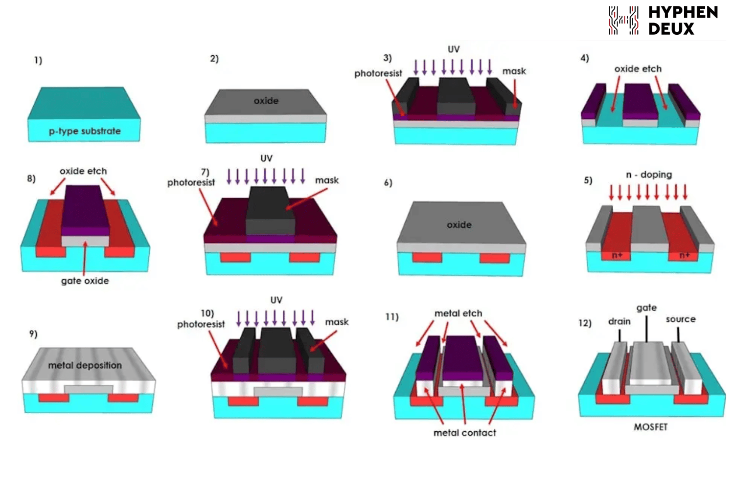
Schematic summary of the major processing steps in the fabrication of a semiconductor device: 1) p-type substrate wafer, 2) thermal oxidation, 3) photolithography, 4) oxide etching, 5) n+ ion implantation, 6) thermal oxidation, 7) gate photolithography, 8) gate oxide etching, 9) metal deposition, 10) metal contact photolithography, 11) metal etching, and 12) final device.
Trends and Innovations in Semiconductor Manufacturing
The semiconductor industry thrives on constant technological advancements, particularly in core processes like pattern transfer, doping, deposition, etching, and packaging. These developments not only address key challenges but also create opportunities for enhanced performance, smaller device sizes, and more efficient production methods.
1. Pattern Transfer: Advancing Lithography
Innovations in lithography, such as extreme ultraviolet (EUV) technology, have been game-changers, allowing the creation of patterns with features as small as a few nanometers. This advancement has fueled the miniaturization of electronic components and is essential for the production of modern microprocessors. Multi-patterning techniques further push the boundaries of precision by creating smaller, more complex patterns than previously achievable.
2. Doping: Precision and Material Innovation
The advent of new materials for doping, such as germanium and arsenic, has expanded the capabilities of semiconductors. Furthermore, the precision of doping techniques, including molecular beam epitaxy (MBE) and CVD, has improved, enabling the creation of more advanced components with optimal electrical properties.
3. Deposition: New Frontiers in Thin Film Technology
Recent breakthroughs in deposition technologies, like metal-organic chemical vapor deposition (MOCVD) and plasma-enhanced techniques, have opened new possibilities for creating highly efficient, high-performance semiconductors. These methods ensure uniform deposition, even on the most complex structures.
4. Etching: Precision and Selectivity
Dry etching techniques such as reactive ion etching (RIE) and plasma etching now offer the precision and control needed for today’s advanced devices. These methods enable the creation of fine features while minimizing damage to adjacent structures, an essential factor in creating high-density integrated circuits.
5. Packaging: Smaller, Faster, and More Efficient
Packaging innovations like 3D stacking, fan-out packaging, and System-in-Package (SiP) are revolutionizing semiconductor design. These methods offer significant advantages, including reduced size, improved performance, and lower power consumption—critical factors in industries ranging from consumer electronics to automotive systems.
The semiconductor manufacturing industry is in a constant state of evolution, driven by increasing demand for smaller, faster, and more efficient devices. While the complexity and costs associated with manufacturing are ongoing challenges, advancements in technology present boundless opportunities for growth. As manufacturers continue to push the limits of what is possible, the industry will be a driving force behind innovations that redefine the way we live and work.
By embracing cutting-edge technologies and optimizing production processes, semiconductor companies stand at the forefront of the next wave of technological transformation—one that holds promise not just for electronics but for industries worldwide, from healthcare to automotive to industrial automation.
About Hyphen Deux
Introducing Hyphen Deux, a cutting-edge startup leading semiconductor progress in Vietnam! We’re the leading fabless design house in Vietnam with a highly experienced international team doing any mixed-signal, digital, embedded, or microcontroller chipset designs to deliver silicon solutions to our customers.
Hyphen Deux is ready to support the development process from concept to ASIC (Application-specific integrated circuit) at any stage and in every inch of specification capture, design, layout, verification and integration, manufacturing, and logistics. Developing MCU (Microcontroller), AI processor, and Healthcare Software, changing the game in the ASEAN semiconductor market.
Source: Semiconductor Engineering
 Navigating Challenges, Embracing Growth